Multiple supply-chain sources confirmed across August 14–17 that NVIDIA will skip TSMC's N2 process family for its post-Rubin 「Feynman」 GPU generation and go straight to the more advanced A16 1.6nm node, with backside power delivery, 3D chiplets via TSMC's System on Integrated Chips (SoIC), custom HBM4E memory, and co-packaged optics (CPO). Mass production is targeted for the second half of 2028, and TSMC is accelerating construction of its AP7 facility in Chiayi and AP8 in the Southern Taiwan Science Park to support a potential 50,000-wafer SoIC monthly run rate by the end of 2027.
Why Skip N2
The leap from Rubin and Rubin Ultra — both on TSMC's N3 family — directly to A16, rather than the more conventional two-step N3 → N2 → A16 cadence, is what makes Feynman distinctive. A16's backside power delivery is the gating feature; combined with TSMC's SoIC 3D chiplet stacking and CoWoS-L 2.5D integration, NVIDIA plans to build multi-kilowatt packages capable of 「dozens of petaFLOPS,」 per TechPowerUp's August 14 analysis of the DigiTimes supply-chain report. Reports from Cnyes on March 22 also suggested some Feynman dies could end up on N3P if supply constraints bind, though NVIDIA has not officially disclosed the per-die allocation.
The Memory and Optical Bets
Feynman will be the first NVIDIA architecture to use a customized HBM4E design with a specialized base die capable of holding logic elements such as memory controllers or packet processing units — effectively pre-processing data before it enters the memory array. The other big bet is co-packaged optics: copper interconnects cannot carry the bandwidth a multi-petaFLOPS package needs, so NVIDIA will move to TSMC's COUPE silicon-photonics platform. The 「Blackwell」 NVL72 rack already does 130 TB/s of GPU-to-GPU bandwidth; Rubin doubles that to 260 TB/s, Rubin Ultra doubles it again to 520 TB/s, and Feynman — by CPO alone — crosses 1,000 TB/s, breaking into the petabyte-per-second class for the first time.
What TSMC Is Doing to Keep Up
TSMC has raised its 2026 capital expenditure to $60–64 billion, with 70–80 percent earmarked for advanced process and packaging capacity. A16 is targeted to reach mass-production readiness in the second half of 2026, and TSMC said on its Q2 2026 earnings call that N2 already accounts for 3 percent of wafer revenue and is set to ramp sharply in the second half. Whether TSMC can allocate enough A16 volume to satisfy NVIDIA's per-die mix is the open question. TSMC's statement that it 「does not anticipate bottlenecks in ramping up capacity」 pertains to the expansion plan itself — not to the allocation question that any single customer cares about.
What It Means for the AI Supply Chain
Feynman's H2 2028 timing puts NVIDIA two years past Rubin's H2 2025 mass production and roughly two years ahead of the next expected A16 customer cycle, which keeps NVIDIA as the public A16 benchmark through at least 2028. The other near-term consequence is for HBM: NVIDIA's custom HBM4E base-die work effectively forces SK hynix, Samsung, and Micron to ship differentiated memory for the first time since HBM2, instead of commodity-spec parts. By 2028, NVIDIA will own the most aggressive co-packaged-optics deployment in any merchant accelerator, and the petabyte-per-second rack class becomes the design point competitors have to clear.
Related Articles
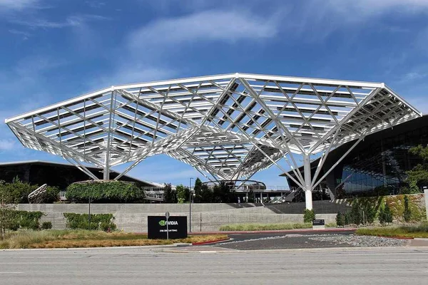
NVIDIA's $50 Billion 13F Reveals Equity Stakes in SpaceX and Intel — and Exclusive Chip-Buyer Commitments in Return
NVIDIA's August 14, 2026 SEC 13F filing discloses $21 billion in SpaceX equity and $30 billion in Intel stock, the same two companies pledging exclusive chip purchases from NVIDIA in prior private agreements. The disclosures turn what was rumor into a confirmed $51 billion cross-equity network.
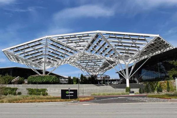
Nvidia Discloses $63.4 Billion in US Equities as Zotac Parent Warns GPU Prices Will Keep Rising
Nvidia's latest 13F filing on August 15 showed it holds $63.44 billion in US-listed equities, with Intel and SpaceX making up 80.3 percent of the portfolio, while Zotac's parent warned of further GPU price hikes through the rest of 2026.
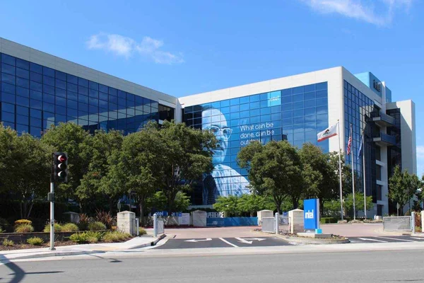
Intel Raises $20 Billion in Upsized Share Sale to Fund Foundry Build-Out
Intel raised $20 billion from an upsized equity offering priced at $95 a share on August 11, cashing in on a stock that has nearly tripled this year to fund its costly contract chipmaking push.
Comments (0)
Log in or sign up to leave a comment.
No comments yet. Be the first to share your thoughts.